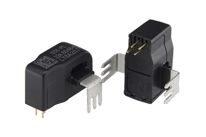
STK-PL/AG

The STK-PL/AG series is based on TMR (Tunneling-Magnetoresistance) technology and open-loop design. It is suitable for DC, AC, pulsed and any kind of irregular current measurement under the isolated conditions. The nominal current range of the STK-PL/AG current sensor consists of 10 A, 20 A, 32 A, 40 A, 50 A.

  • Product Features
  • Typical Application
Product Features
  • Typical applications
     PV combiner box
     PV inverter (MPPT & AC)
     motor driver controller
     SMPS & UPS
     Battery management system
  • Limit Parameters
  • Electrical Parameters(Ta=25℃)
  • Physical Parameters
  • Parameter

    Symbol

    Unit

    Min

    Typ

    Max

    Comment

    Primary nominal current rms

    I_pn

    A


    10


    Primary current measuring range

    I_pm

    A

    -25


    25


    Supply voltage

    Vcc

    V

    4.75

    5

    5.25


    Current consumption

    Icc

    mA


    5

    10


    Reference voltage

    Vref

    V

    2.48

    2.5

    2.52

    Output function

    Rated output voltage

    V_FS

    V


    0.8


    (Vout - Vref )@ I_pn

    Internal output resistance

    R_out

    Ω


    1


    Output

    Internal output resistance

    R_ref

    Ω


    1


    Output

    Quiescent voltage

    Voff

    V

    2.48

    2.5

    2.52

    Vout @ 0 A

    Electrical offset voltage

    Voe

    mV

    -10


    10

    (Vout – Vref) @ 0 A

    Temperature drift of Voe

    Voe_TRange

    mV

    -8


    8

    -40 ~ 105

    Magnetic offset current

    I_om

    A

    -0.25


    0.25

    @ ±10 x I_pn

    Theoretical gain

    G_th

    mV/A


    80


    800 mV @ I_pn

    Error of gain

    Err_G

    %G_th


    ±0.5


    Trimmed in the factory @ 25

    Temperature drift of gain

    G_TR

    %G_th

    -1.0


    1.0

    -40 ~ 105

    Rated linearity error

    Non-L_pn

    %I_pn

    -0.5


    0.5

    ±I_pn

    Linearity error @ I_pm

    Non-L_pm

    %I_pm

    -1


    1

    ±I_pm

    Reaction time

    t_ra

    µs


    0.1

    0.2

    @ 10% of I_pn

    Step response time

    t_res

    µs


    0.2

    0.5

    @ 90% of I_pn

    Delay time

    t_delay

    µs


    0.2


    1000kHz sine wave

    Frequency bandwidth (-3dB)

    BW

    kHz


    1000


    No RC circuit

    Output voltage noise

    DC ~ 10 kHz

    DC ~ 100 kHz

    Vnoise

    mVpp


    15

    25


    Accuracy @ 25

    X

    % of I_pn

    -1


    1

    @ 25

    Accuracy @ -40 ~ 105

    X_TRange

    % of I_pn

    -2


    2

    -40 ~ 105


  • Mechanical Dimension Drawing(mm)