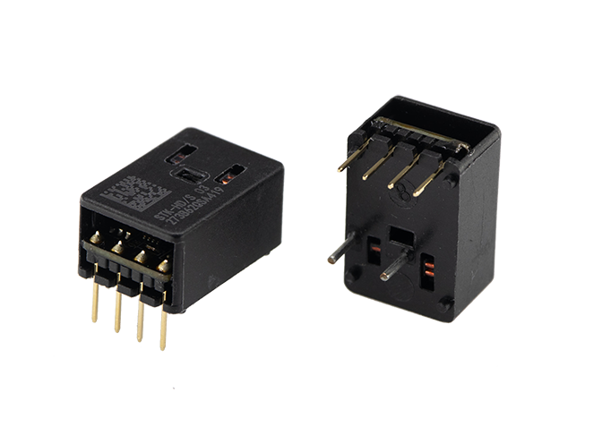
STK-HD/SG

STK-HD/SG current sensor is based on the open loop principle and TMR technology. DC, AC, pulses and any kind of irregularities wave can be measured by the current sensor under the isolated conditions.

  • Product Features
  • Typical Application
Product Features
  • AC Variable speed drives

    Direct-current dynamo

    Servo driver

    MPPT

    Switched model power supplies (SMPS)

  • Limit Parameters
  • Electrical Parameters(Ta=25℃)
  • Physical Parameters
  • Parameter

    Symbol

    Unit

    Min

    Typ

    Max

    Comment

    Primary nominal current rms

    I_pn

    A


    15


    Supply voltage

    Vcc

    V

    4.75

    5

    5.25


    Current consumption

    Icc

    mA


    5

    10


    Reference voltage

    Vref

    V

    0.47

    0.5

    0.53

    Output function

    Quiescent voltage

    Vout @ 0 A

    Voff

    V

    0.47

    0.5

    0.53


    Electrical offset voltage

    (Vout – Vref) @ 0 A

    Voe

    mV

    -8


    8


    Rated output voltage

    ((Vout – Vref)@I_pn) – Voe

    V_FS

    V


    3.75


    Internal output resistance

    R_out

    Ω


    1


    Internal reference resistance

    R_ref

    Ω


    1


    Theoretical gain

    G

    mV/A


    250


    Rated linearity error

    Non-L

    %I_pn


    0.5


    Within ±I_pn

    Step response time

    t_res

    µs


    0.4


    @ 90% of I_pn

    Frequency bandwidth (-3dB)

    BW

    kHz


    600


    No RC circuit

    Output voltage noise

    DC ~ 10 kHz

    DC ~ 100 kHz

    Vnoise

    mVpp


    1

    4


    @250kHz

    Sampling Rate

    Accuracy @ 25

    X

    % of I_pn

    -0.8


    0.8

    @ 25

    Accuracy @ -40~105

    X_TRange

    % of I_pn

    -1.5


    1.5

    -40 ~ 105

  • Mechanical Dimension Drawing(mm)